3D printed active electronics
MIT researchers have demonstrated a completely 3D printed semiconductor-free resettable fuse.
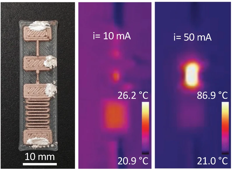
Fabricated using standard 3D printing hardware and inexpensive biodegradable polymer filaments doped with copper nanoparticles, the device has the same switching characteristics as semiconductor-based transistors used in active electronics processing operations. function can be performed. Even after 4,000 switching cycles, the device showed no signs of degradation.
Although it lacks the performance and small size of semiconductor transistors, the researchers said the 3D-printed devices could be used for basic control operations such as regulating the speed of electric motors.
The device is made from thin 3D-printed traces of copper-doped polymer. They contain intersecting conductive regions that allow researchers to tune the resistance by controlling the voltage supplied to the switch. (Credit: Image provided by researchers / MIT)
“This technology has real legs. It cannot compete with silicon as a semiconductor, but our idea is not necessarily to replace what already exists, but to push 3D printing technology into uncharted territory. In a nutshell, this is really about the democratization of technology, potentially allowing anyone to create smart hardware far from traditional manufacturing centers.” said Luis Fernando Velazquez García, principal investigator at MIT’s Microsystems Technology Laboratory. “The reality is that there are many engineering situations where you don’t need the best chips. At the end of the day, all you care about is whether the device can perform the task. This technology is capable of meeting those constraints. can.”
The researchers aim to further develop the technology to print fully functional electronics and produce working magnetic motors using only extrusion 3D printing. (1)
Edible toothpaste-based transistor
Researchers from the Italian Institute of Technology and the University of Novi Sad have designed an edible toothpaste-based transistor that could be used in applications such as smart pills.
This device is made of copper phthalocyanine. Copper phthalocyanine is a food-grade blue pigment that acts as a whitening agent in some toothpastes. The chemical structure of the pigment facilitates charge conduction within the crystal. Approximately 10,000 transistors would be manufactured based on the amount ingested while brushing teeth.
In addition to copper phthalocyanine, the researchers used an ethylcellulose substrate for their edible circuit, and the electrical contacts were printed using inkjet technology and a solution of gold particles common in food decoration. A “gate” made of an electrolytic gel based on chitosan (a food-grade gelling agent derived from crustaceans) allows the transistor to operate at low voltages of less than 1V.
The research team plans to identify other edible substances with suitable chemical and physical properties to create edible electronic devices that can be used for medical applications such as monitoring body parameters in the gastrointestinal tract. (2)
Solution deposition of large electronics
Researchers at the University of Illinois at Urbana-Champaign have proposed a new solution deposition process for semiconductors that creates higher-performance transistors by introducing more defects.
The researchers used solution deposition of the ordered defect compound semiconductor copper indium selenium (CuIn5Se8) to form high-speed logic circuits that operate at megahertz and have delays of up to 75 nanoseconds. This process was also used to create a transistor that drives an inorganic microLED-based microdisplay with a resolution of 508 pixels per inch.
“Remarkably, despite having more defects, they are organized into ordered defect pairs, which makes our material a record high for materials produced by solution deposition processes. “That’s why it has such high performance,” said Qing Cao, associate professor of materials science and engineering at the university. Granger Institute of Technology, University of Illinois at Urbana-Champaign. “We have shown that we can go beyond basic materials science to build functional circuits and systems such as displays, paving the way for adoption in many emerging applications that require high-performance electronics covering a wide range of areas. I did.”
The material’s mobility is 500 times higher than the amorphous silicon semiconductors used in large LCD displays and four times higher than the metal oxide semiconductors used in organic LED displays. The mobility is comparable to low-temperature polycrystalline silicon used in smartphone displays, and there is no need for the laser annealing process that limits display size. Next, the researchers hope to make the process more environmentally friendly. (3)
References
(1) Canadada, J., Velasquez García, LF (2024). Monolithically 3D printed logic gates and resettable fuses without semiconductors. Virtual and Physical Prototyping, 19(1). https://doi.org/10.1080/17452759.2024.2404157
(2) E. Feltri, P. Mondelli, B. Petrović, FM Ferrarese, A. Sharova, G. Stojanović, A. Luzio, M. Caironi, Completely edible transistors based on toothpaste dyes. Advanced science. 2024, 2404658. https://doi.org/10.1002/advs.202404658
(3) Hsien-Nung Wang et al., Solution-processable ordered defect compound semiconductors for high-performance electronics. Science. Advanced 10, eadr8636 (2024). https://doi.org/10.1126/sciadv.adr8636
Jesse Allen
(All posts)
Jesse Allen is the Knowledge Center Administrator and Senior Editor for Semiconductor Engineering.
Source link

